


Plating of Semiconductor Packages
The manufacturing processes of semiconductors can be broadly divided into front-end processes,
in which the circuit is formed on the wafer, and back-end processes, in which the IC chips are cut out, wired, and packaged.
Plating is an indispensable technology used in package substrate mounting, which is part of the back-end processes.
In this chapter, we will learn about the plating technologies used in semiconductor packaging.
What kinds of semiconductors use plating?
Semiconductors are installed in many different products in our daily lives, including smartphones, tablets, PCs, refrigerators, washing machines, cameras, photocopiers, and automobiles. They play a role in controlling voltage and electric current, as well as in memory storage and calculation. It would no longer be an exaggeration to say that our lives would be impossible without semiconductors.
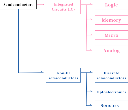
According to the World Semiconductor Trade Statistics (WSTS) definitions, there are two broad categories of semiconductors: Integrated Circuits (IC) and other semiconductors. ICs are further divided into four sub-categories of Logic, Memory, Micro, and Analog, and non-IC semiconductors into three sub-categories, namely Discrete Semiconductors, Optoelectronics, and Sensors.
The types of plating used in integrated circuits (IC) include bump plating, which achieves multidimensional mounting of Logic and Micro ICs, redistribution layer (RDL) plating, and copper pillar plating.
Plating is also used in lamination wiring process and final surface treatment of the package substrate on which the ICs are mounted. It is also used in Analog ICs on organic substrates on which power management ICs (PMICs) are mounted.
In the other semiconductors category, plating is used on wafers in power semiconductors, which are classified as Discrete Semiconductors. We will learn about power semiconductors in Chapter 6. Plating is also used on wafers in Optoelectronics and Sensors.

Where on package substrates is plating used?
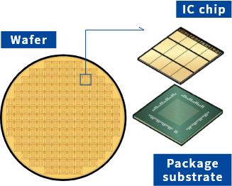
Today, silicon is the predominant material used to make semiconductors. Wafers are made by slicing a single-crystal ingot of silicon into wafers, which are circular plates of about 1 mm. In the front-end process of semiconductors, circuit patterns are created on the surface of these wafers.
In the back-end process, these wafers are cut into IC chips that range in size from a few millimeters to less than 20 mm square. These chips are then incorporated into the package substrate. The roles of the package substrate are to protect the IC chips from water and dirt and to facilitate mounting (adhering) onto the printed circuit board.
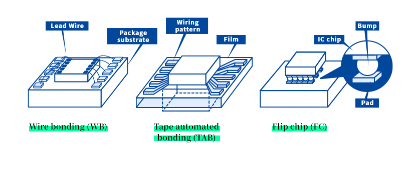
There are three ways to connect the external terminals of the IC chips and the package substrates electrically: wire bonding (WB), tape automated bonding (TAB), and flip chip (FC).
Flip chip is currently the predominant mounting method used for high-performance devices. Flip-chip ball grid array (FC-BGA) substrates, which are made with the flip chip method, are used in a wide range of applications, including servers, smartphones, and PCs.

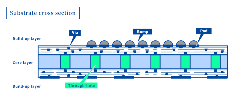
The core layer of a FC-BGA substrate is made of a copper-clad laminated plate (plate made by adhering copper foil and resin substrate). Many holes are drilled in this core layer at pre-defined positions, and to connect both sides electrically, the inner surfaces of these holes are plated using electroless copper plating, followed by electrolytic copper plating of the required thickness. The copper plating that connects these layers is known as through-hole plating.
A film of insulating material is then layered on both sides of the core layer, a laser is used to drill holes (vias) to connect the layers, and a circuit is formed by the copper plating. This process is repeated multiple times to create build-up layers.
To finish, the package is coated with a solder resist (insulating film to protect the circuit pattern), followed by final surface treatment of the terminals. The purpose of final surface treatment is for the solder to coat (wet) and bond to the terminal surface, making the bond less susceptible to deterioration in the operating environment. Depending on the application, a variety of treatments are used for this final surface treatment, including electroless nickel/palladium/gold plating (ENEPIG).

In this chapter, we have learned about the plating technologies used primarily for package substrate mounting, which is part of the back-end process of semiconductor manufacture. With the growing sophistication of semiconductor devices, package substrate mounting now requires minimization of wire widths and via diameters, uniformity of conductor film thickness, and maintenance of solder bond reliability. Plating technology play a crucial role in realizing these properties.