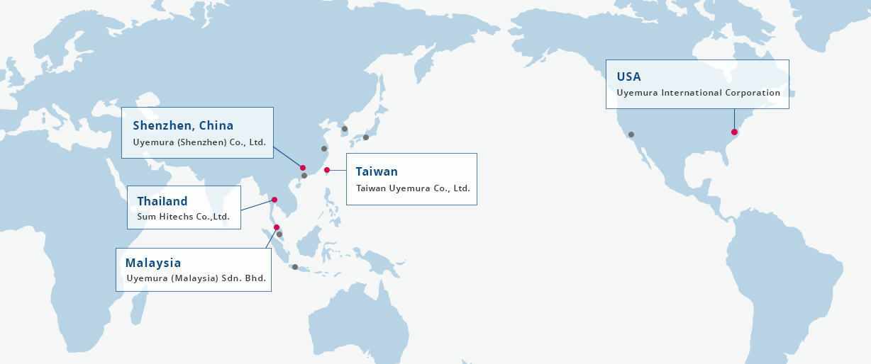
If we add together all our engineering and machine design staff, nearly half of all the employees of Uyemura are engaged in development and engineering support work. The aim is for the research laboratory to provide a space where those many employees can come together and new discussions and free thinking will occur, to lead to the creation of new value and the advancement of our technological strength.
The laboratory contributes to the further advancement of plating technology as a world-leading academic research institution that combines the research abilities and technical abilities created from free thinking with the experimental facilities necessary to make high level research and development possible. It also provides a unique service to our customers.
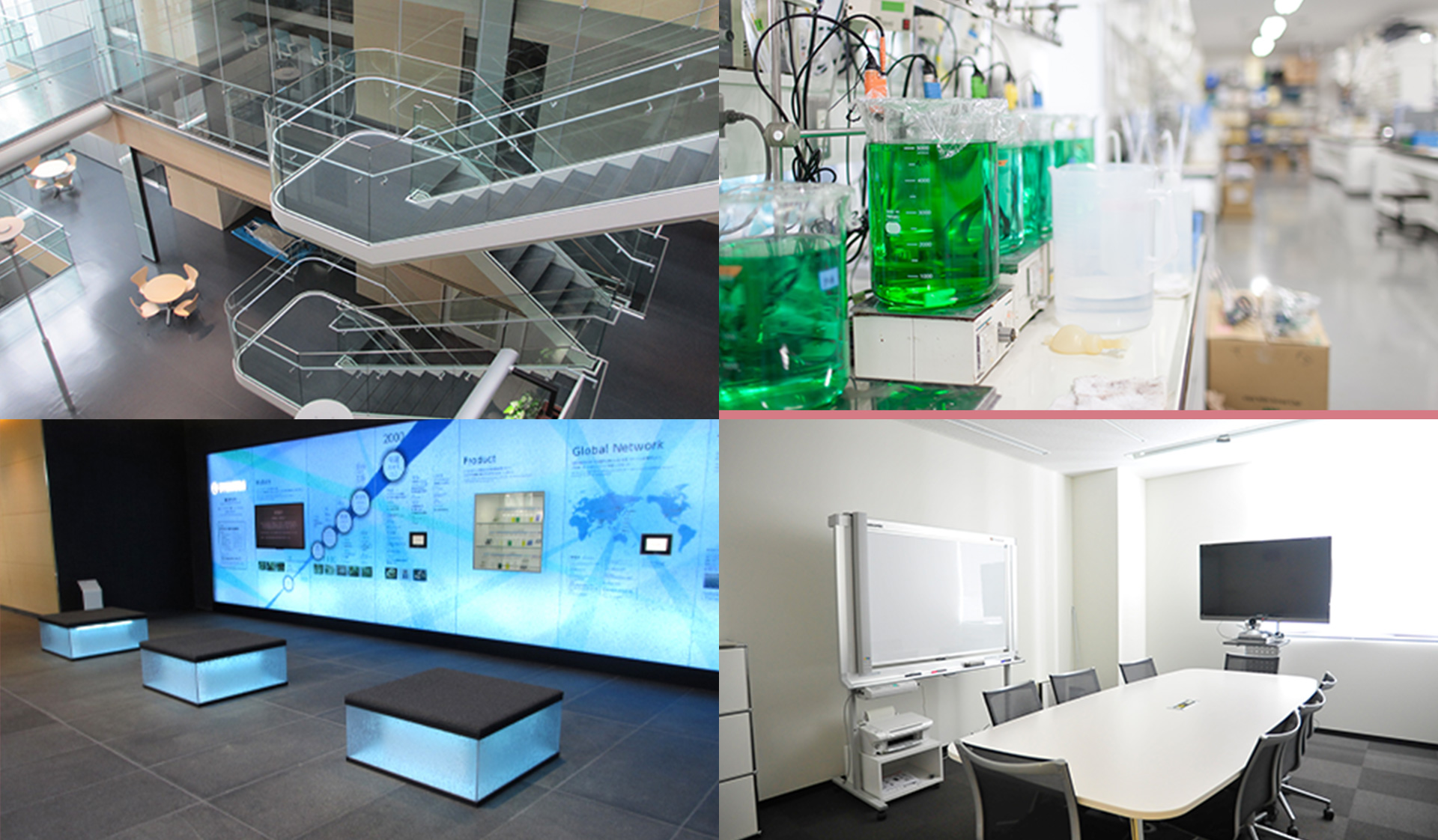
The research and development system at Uyemura
Research activities are truly the driving force for Uyemura.
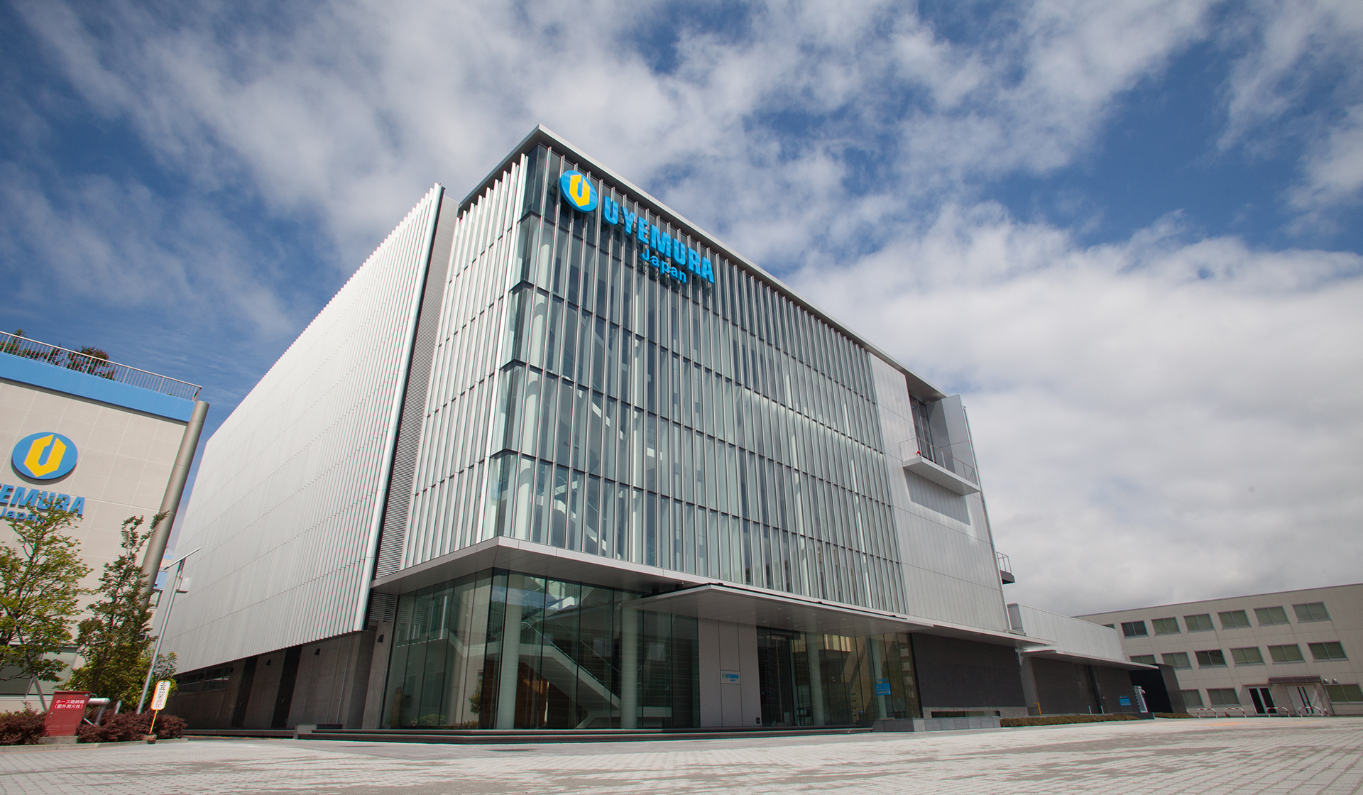
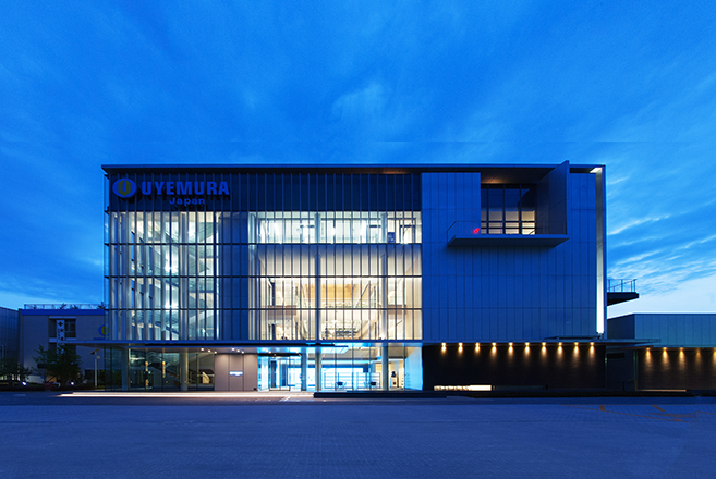
Central Research Laboratory
The technical capabilities of Uyemura as an “all-round manufacturer for surface treatment” are supported by our Central Research Laboratory in Osaka, Japan. This was established in 1968 as a laboratory specializing in plating.
The laboratory has the analysis equipment necessary to make the high level analysis possible and one of the best collections of specialist materials in Japan. It performs research and development into surface treatment technologies that combine chemicals, mechanics and electronics.

Facilities for experiments
In addition to normal line laboratories, we have ample laboratories for each separate development department. This includes four line laboratories in a cleanroom environment, two rooms for the trial production of sample liquids and laboratories for joint experiments with customers.
We also have another research building which is equipped with the latest types of plating equipment and maintain around 250 individual analytical instruments, including TEM, FIB-SEM and XPS. We put full effort into new chemical development and the solution of problems for customer support.

Example analysis equipment TEM 
JEM-F200 made by JEOL Ltd.
This is equipment synonymous with high-resolution observation in microscopic areas. Elemental analysis has become possible with the atomic arrangement of the plating film and the accompanying EDS, enabling nano-level observation of the state of the plating film and the film interface.
FIB-SEM 
XVision 210B made by Hitachi High-Tech Corporation
This is equipment of the highest level in the world. It combines FIB and FE-SEM, both of which continue to show remarkable progress. The use of this equipment makes it possible to observe SEM images without needing to remove the sample from its housing. Furthermore, the use of the attached EDS has also made it possible to perform more detailed elemental analysis.
XPS 
PHI Quantera Ⅱ made by ULVAC-PHI, Inc
This is equipment that can obtain data on the composition and chemical bonding state of a surface by irradiating a sample with X-rays and measuring the energy of the photoelectrons emitted from its surface. This highest level equipment is used for customer support and new product development.
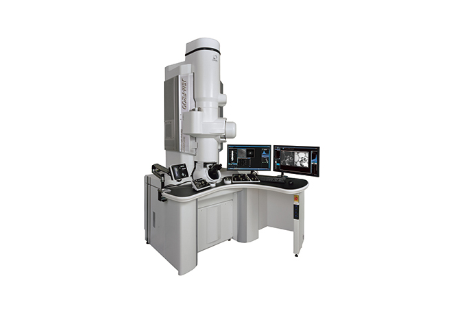
JEM-F200 made by JEOL Ltd.
This is equipment synonymous with high-resolution observation in microscopic areas. Elemental analysis has become possible with the atomic arrangement of the plating film and the accompanying EDS, enabling nano-level observation of the state of the plating film and the film interface.
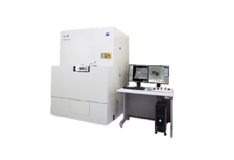
XVision 210B made by Hitachi High-Tech Corporation
This is equipment of the highest level in the world. It combines FIB and FE-SEM, both of which continue to show remarkable progress. The use of this equipment makes it possible to observe SEM images without needing to remove the sample from its housing. Furthermore, the use of the attached EDS has also made it possible to perform more detailed elemental analysis.
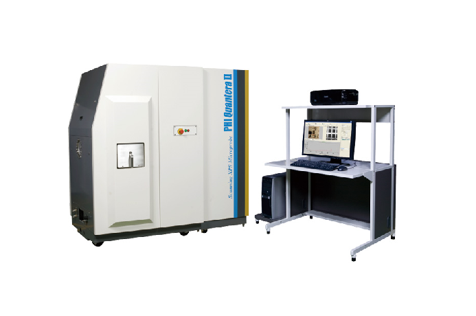
PHI Quantera Ⅱ made by ULVAC-PHI, Inc
This is equipment that can obtain data on the composition and chemical bonding state of a surface by irradiating a sample with X-rays and measuring the energy of the photoelectrons emitted from its surface. This highest level equipment is used for customer support and new product development.
Environmentally-symbiotic laboratory
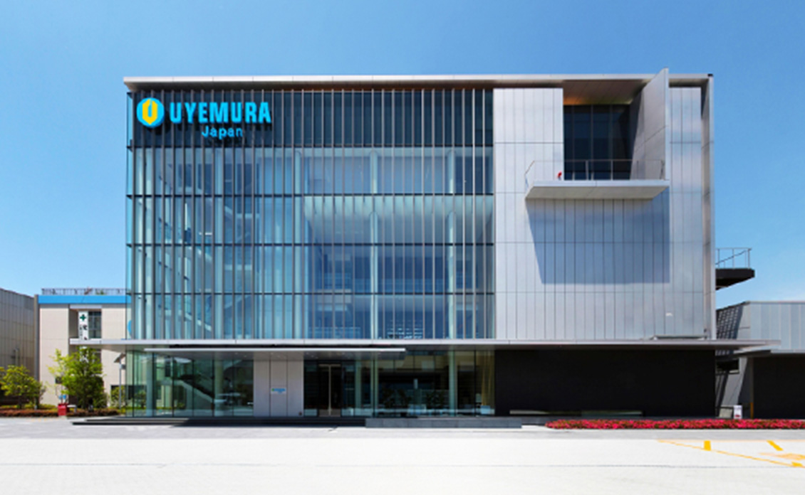
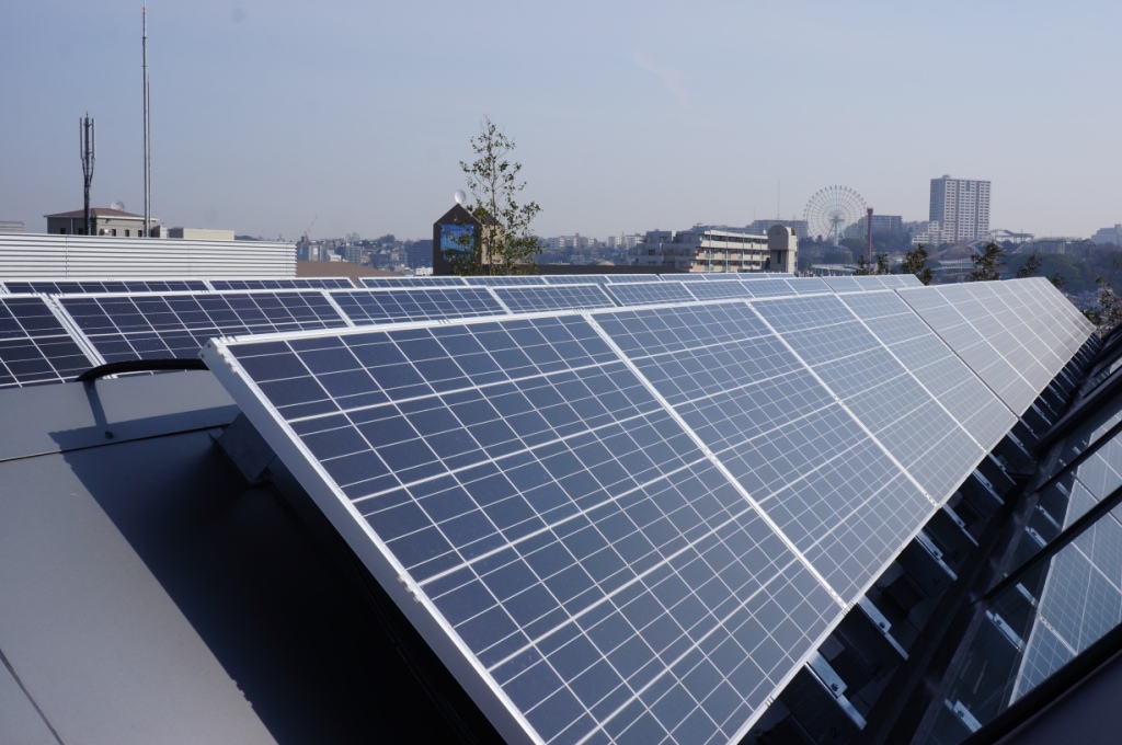
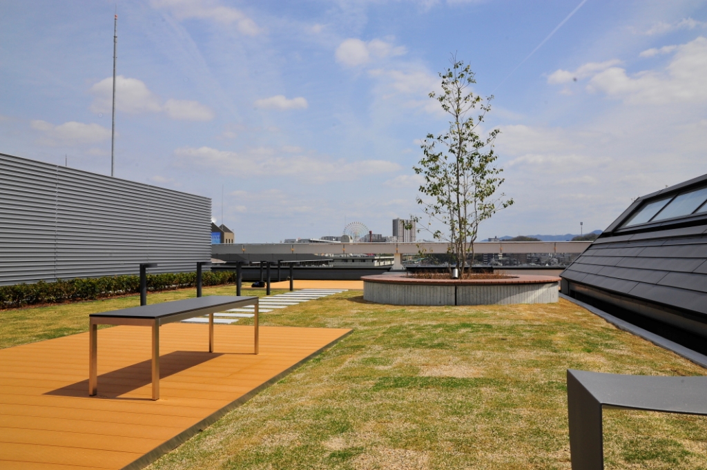
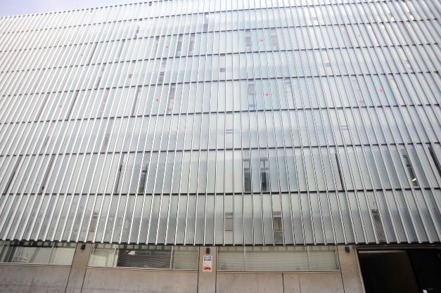
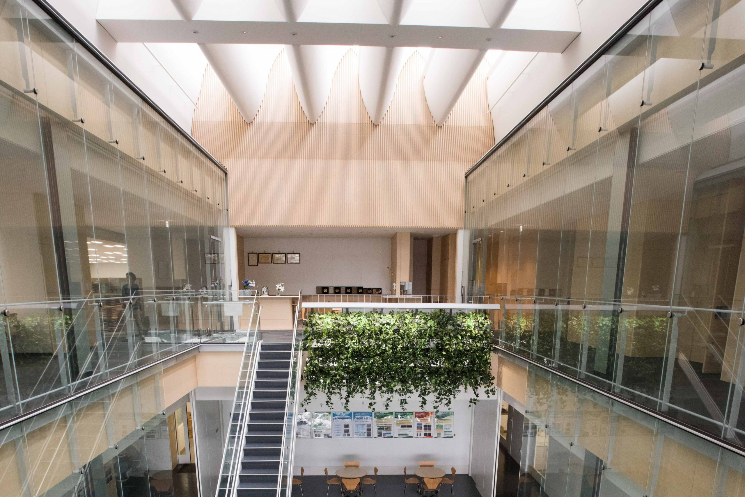
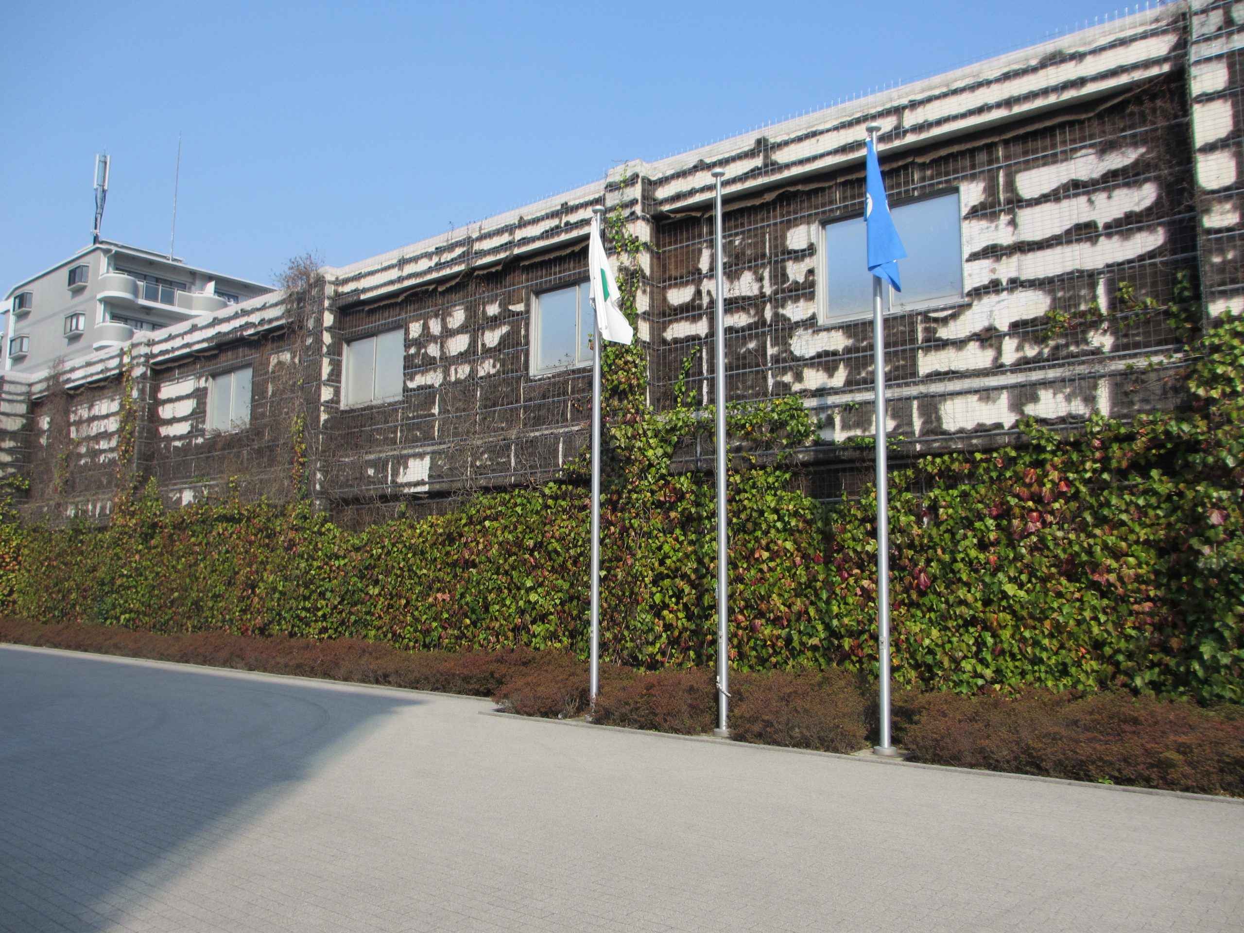
The Central Research Laboratory building, completed in 2013, incorporates the concept of environmentally friendly design and received the highest S rank (ranked second out of 148 buildings with a floor area of over 5,000 square meters for which a green building plan was submitted to Osaka Prefecture in FY2011) from CASBEE (Osaka Prefecture's Comprehensive Assessment System for Built Environment Efficiency).
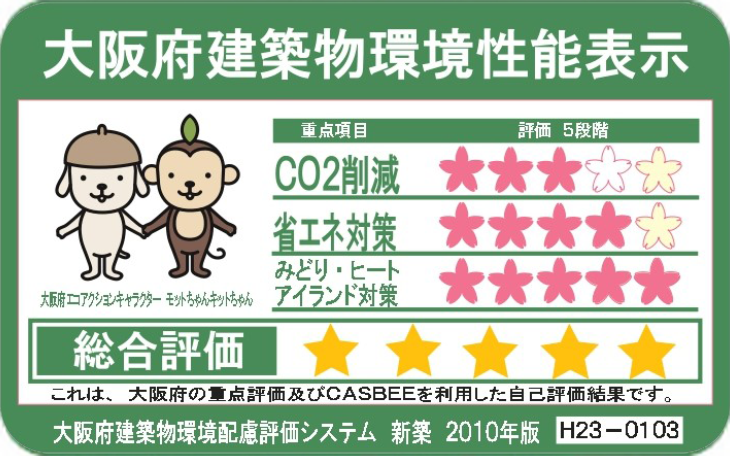
Major environmentally friendly initiatives
Association with SDGs
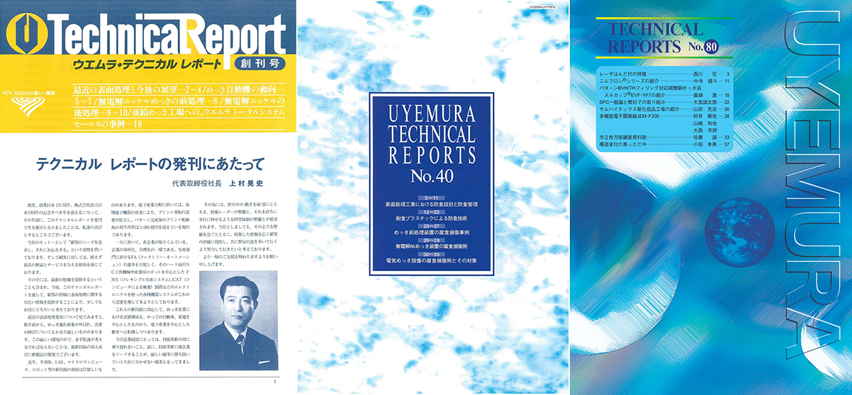
UYEMURA TECHNICAL REPORTS
This was first published in 1983 as a result of our desire to be of use to the customers and our motto to “Pursue the requirements of the customers and respond to them.” It offers a wide range of the latest information related to surface treatments. As part of our paperless efforts, the reports have been available electronically since 2021.
R&D Bases at Overseas Subsidiaries
Overseas, we have R&D bases in USA, Taiwan, Malaysia, Shenzhen in China, and Thailand, where we develop products that suit each region. In the future, we will continue to promote our global R&D system that is closely tied to local communities by utilizing our overseas bases, with the Central Research Laboratory in Japan as a central base.

USA
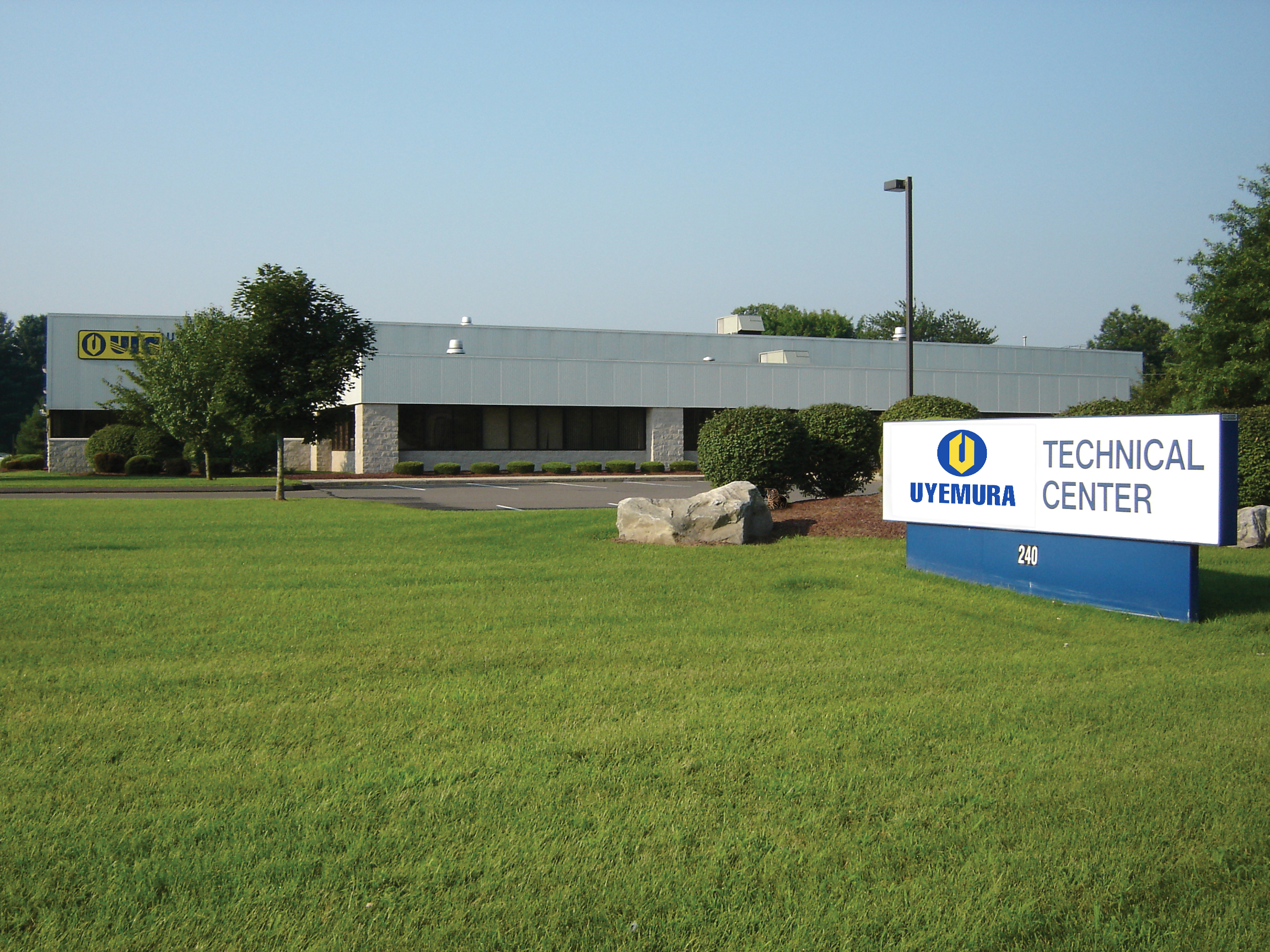
Uyemura International Corporation Technical Center
Uyemura Technical Center was opened in Connecticut, USA in 1998. Its mission is to support Uyemura’s global brand, and to provide early design-phase support and innovative surface treatments to OEMs and customers in the US, Canada, and Mexico.
Uyemura USA senior management provides guidance and leadership to IPC, HDPug and NASF, and actively manages the technical teams that tailor Uyemura processes to customers’ unique requirements.
These activities have generously rewarded Uyemura with the confidence of leading manufacturers in every sector of industry, including printed circuits, semiconductors, semiconductor packages, and medical diagnostics.
Taiwan
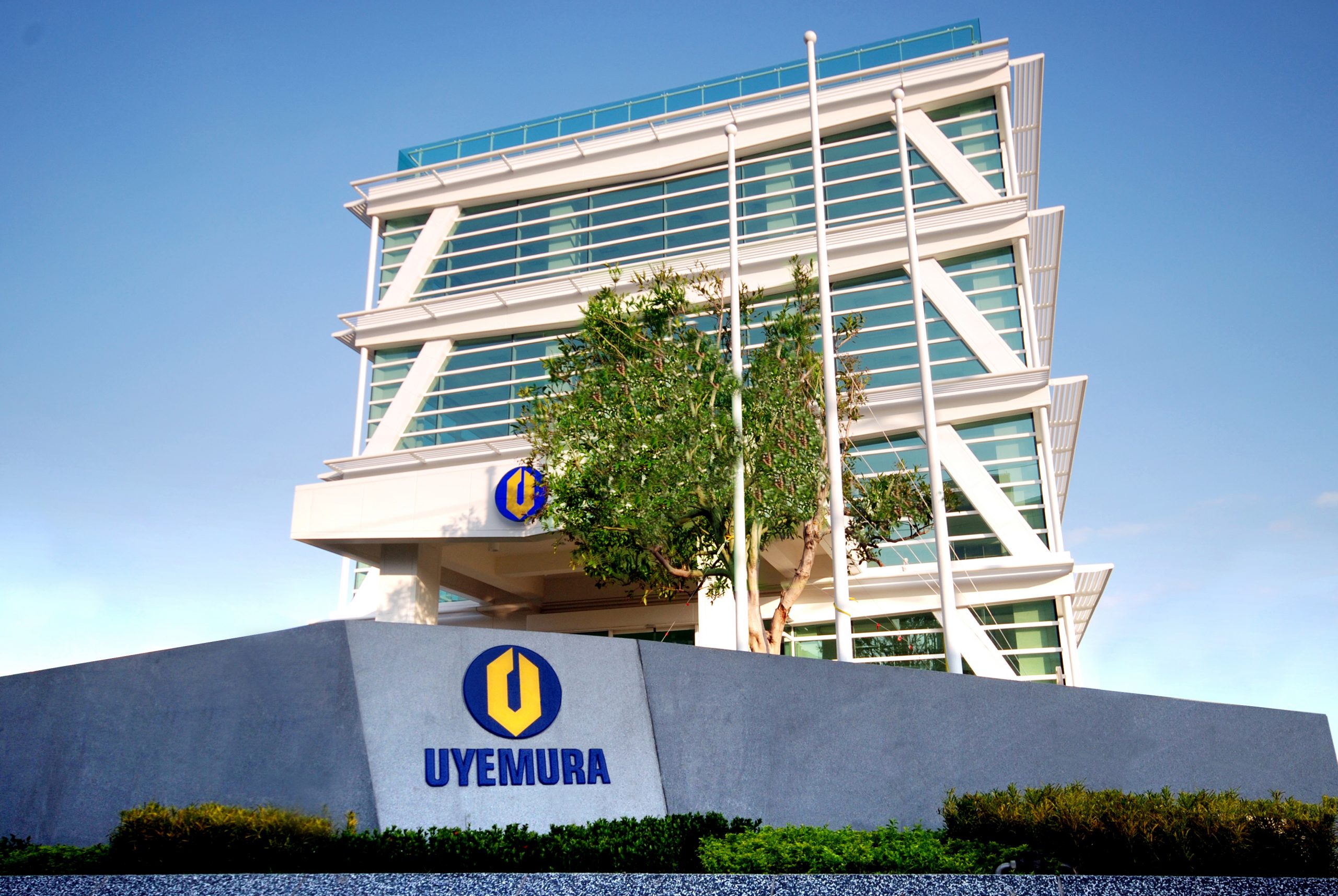
Taiwan Uyemura Co., Ltd. Research Laboratory (TRL)
Since its establishment in 2005, the Taiwan Research Laboratory has complemented the Central Research Laboratory in Japan and worked to respond quickly to the needs of Taiwanese customers. Taiwan Uyemura has an in-house chemical plant, machinery plant, and plating processing plant. Taking advantage of this environment, we are striving to develop not only chemicals but also products with full consideration of plating facilities and actual production.
Malaysia
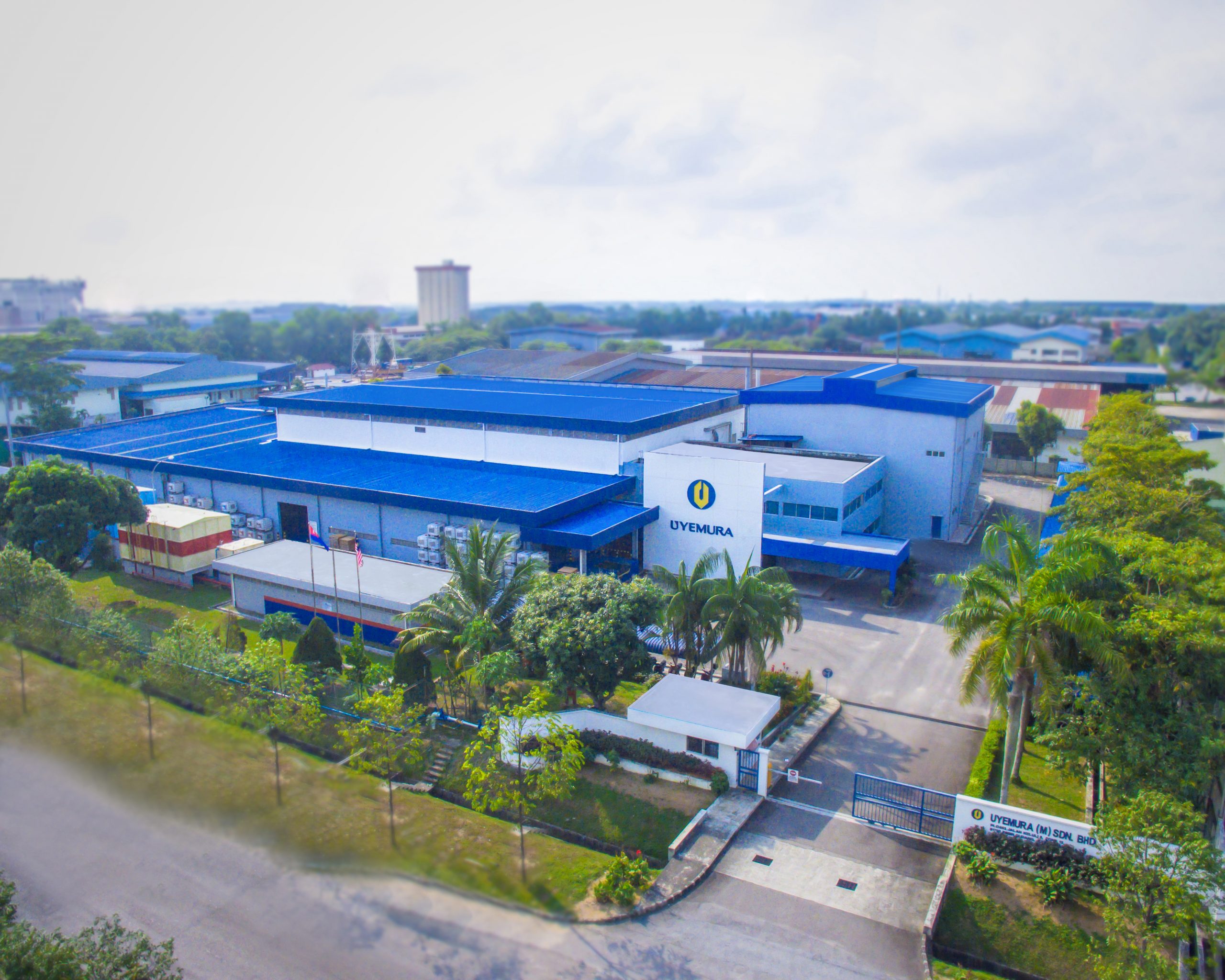
Uyemura (Malaysia) Sdn. Bhd.
Established in 2005, the R&D department develops surface treatment chemicals that are in high demand in the ASEAN market.
R&D activities are steadily expanding, focusing on a wide range of fields, including chrome plating, electroless nickel plating, and other plating technologies.
We have technical partnerships with local universities to enhance innovation and knowledge.
We also provide a wide range of customer-focused technical services to ensure the full performance of our marketed products.
Shenzhen, China
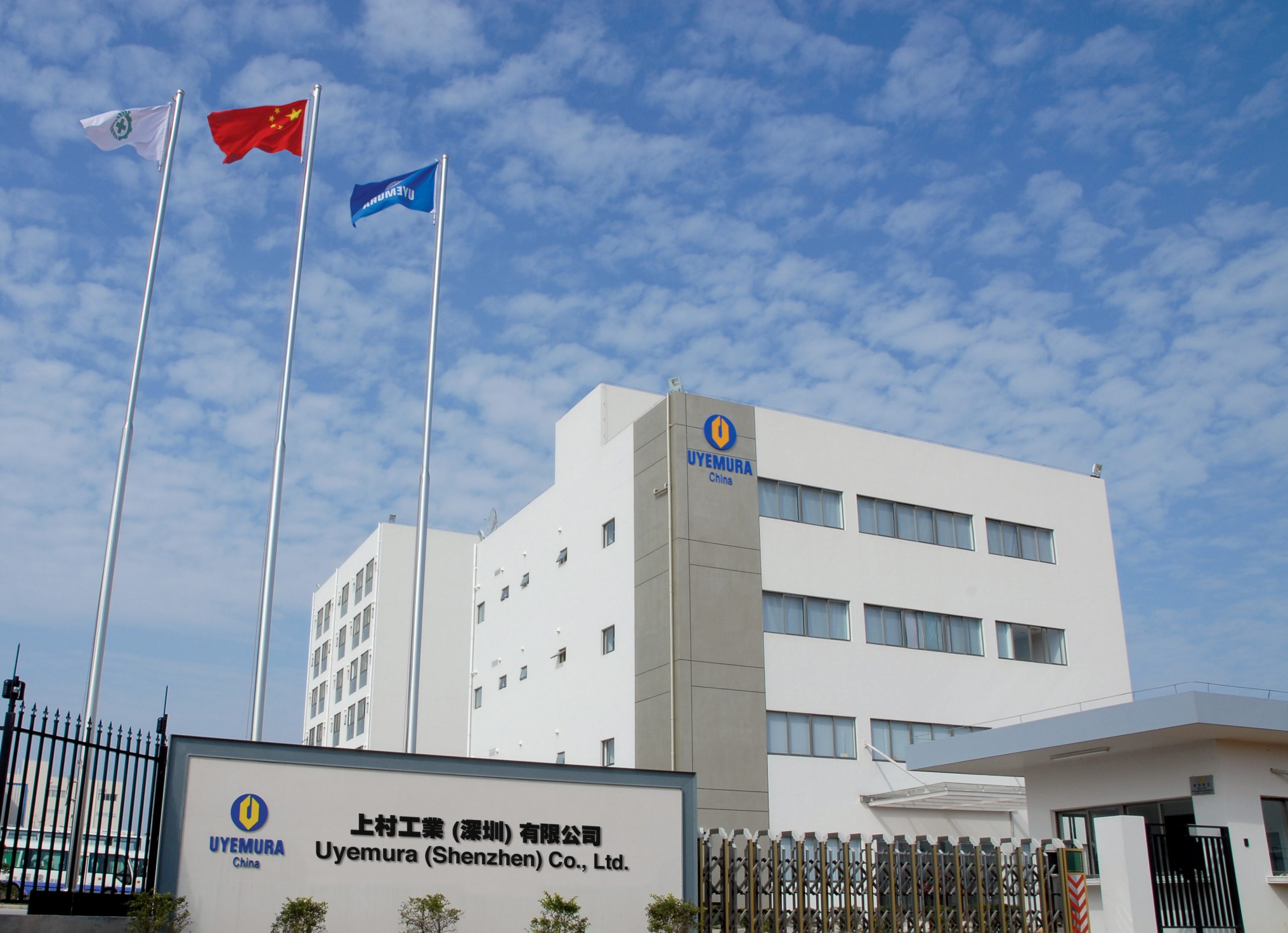
Uyemura (Shenzhen) Co., Ltd.
The company was started with the aim of improving and developing products in accordance with the requirements of users in China. In 2006, along with the opening of our new plant, we established a new development base in Pingshan District, Shenzhen, and are currently developing our own products, mainly using electroless processes, to meet the unique requirements of China.
In 2021, we established a clean room for development so that we can conduct R&D at the level of actual machines not only for chemicals but also for machinery, and are focusing on the development of leading-edge semiconductor-related products.
Thailand
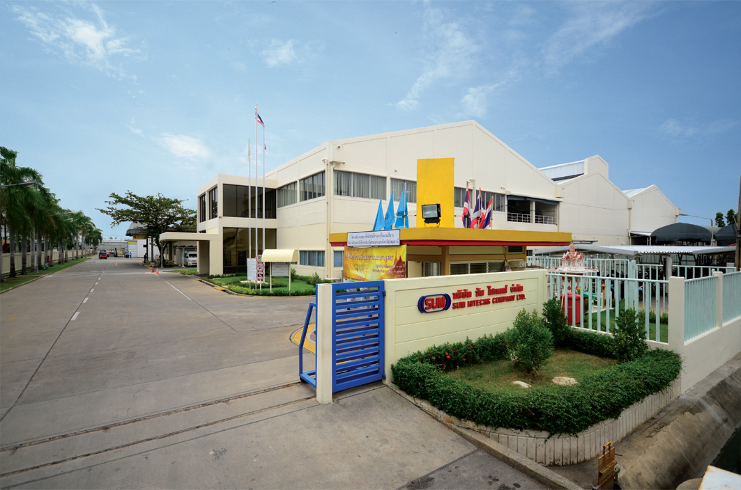
Uyemura (Thailand) Co., Ltd.
The company was established in 1987 to mold, paint, and plate plastic parts for automobiles and home appliances. We also perform decorative plating as well as plating of printed circuit boards.
We are enhancing our system for accumulating information that has been fed back from the field as know-how, and strengthening our support system to solve various problems. In recent years, we have been actively working to expand the possibilities of plating technology, such as plating on complex shapes, by utilizing plating simulation analysis.

